TDR/TDT Characterization
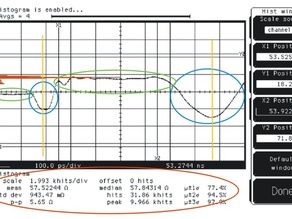
A lot of information can be read from a TDR screenshot. Below is TDR readout of a PCB with a connector at the end.
Using the histogram function (red histogram on the left side of the picture) impedance is evaluated automatically. On the bottom (red ellipse) the measurement result of 57.5 Ohm with the corresponding statistical variation is shown.
The TDR measurement starts with the 50 Ohm cable used to supply the step to the DUT (first green ellipse).
After that, a capacitive dip can be seen (first blue ellipse). If a connector is used to supply the step to the DUT this dip would be caused by the connector. In this particular case a proper RF probe was used avoiding this kind of capacitive load. Here, it is really the pad at the edge of the PCB which causes a capacitive dip. One possible counter measure would be to reduce the size of the ground plane underneath the edge pad.
Next, the 57 Ohm transmission line on the PCB can be seen (second green ellipse, target impedance was 60 Ohm). The length of around 680 ps (left to right yellow bar) is twice the flight time of the signal (as we are measuring the reflection). So the electrical length is around 340 ps. At a signal speed of 6 ps/mm this calculates to around 56 mm physical length.
Finally, there is a last huge capacitive dip (second blue ellipse). This is a SMD SO-DIMM connector with large pads causing high capacitive load. Integrating the area of the dips and peaks, the scope can accurately calculate the size of any capacitor or an inductor on the trace.
Image Gallery
EyeKnowHow
Hermann Ruckerbauer
Itzlinger Straße 21a
94469 Deggendorf
Germany
Phone: +49 991 29692905
Fax: +49 991 98158793
Mobile: +49 176 78778777
Hermann.Ruckerbauer@EyeKnowHow.de


